Columbia engineers have produced a powerful 3D photonic-electronic chip that could overcome one among AI’s biggest hardware challenges: energy-hungry data transfer
Their design integrates light-primarily based data movement with CMOS electronics to accomplish unmatched efficiency and bandwidth. This advancement may want to reshape AI hardware, permitting smarter systems that pass data quicker even as using far less energy—key for future technologies like independent vehicles, large AI models, and more.
Breaking AI’s Energy Barrier
Artificial intelligence (AI) carries the potential to activate important technological advancement, but its development has been slowed by energy inefficiencies and data transfer bottlenecks. Now, researchers at Columbia Engineering have evolved a promising solution: a 3D photonic-electronic platform that dramatically enhances both energy performance and bandwidth density. These are main steps in the direction of building faster, more capable AI hardware.
The work, posted in Nature Photonics and accompanied by Keren Bergman, Charles Batchelor Professor of Electrical Engineering, initiates a novel method that integrates photonics with improved complementary metallic-oxide-semiconductor (CMOS) electronics. This blending permits excessive-speed, energy-efficient data communication and at directly tackles one among AI’s biggest hardware boundaries: transferring big quantities of data quickly without draining power.
Crushing the Data Transfer Limit
“In this work, we introduces a technology able to transferring huge volumes of data with unfamiliar to low energy consumption,” stated Bergman. “This development breaks by the long-standing energy obstacles that has restricted data movement in traditional computer and AI systems.”
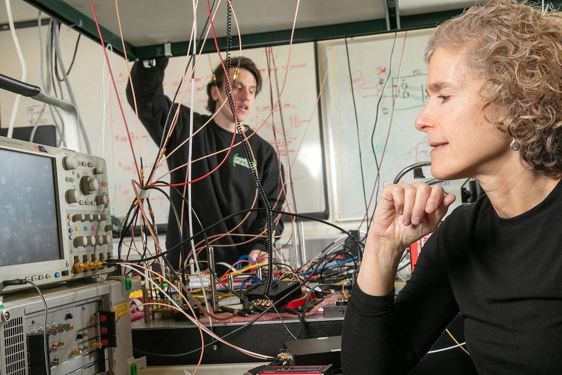
-Michael Cullen, electrical engineering graduate student and co-author of the paper, works with Keren Bergman (foreground) in the Lightwave Research Laboratory.
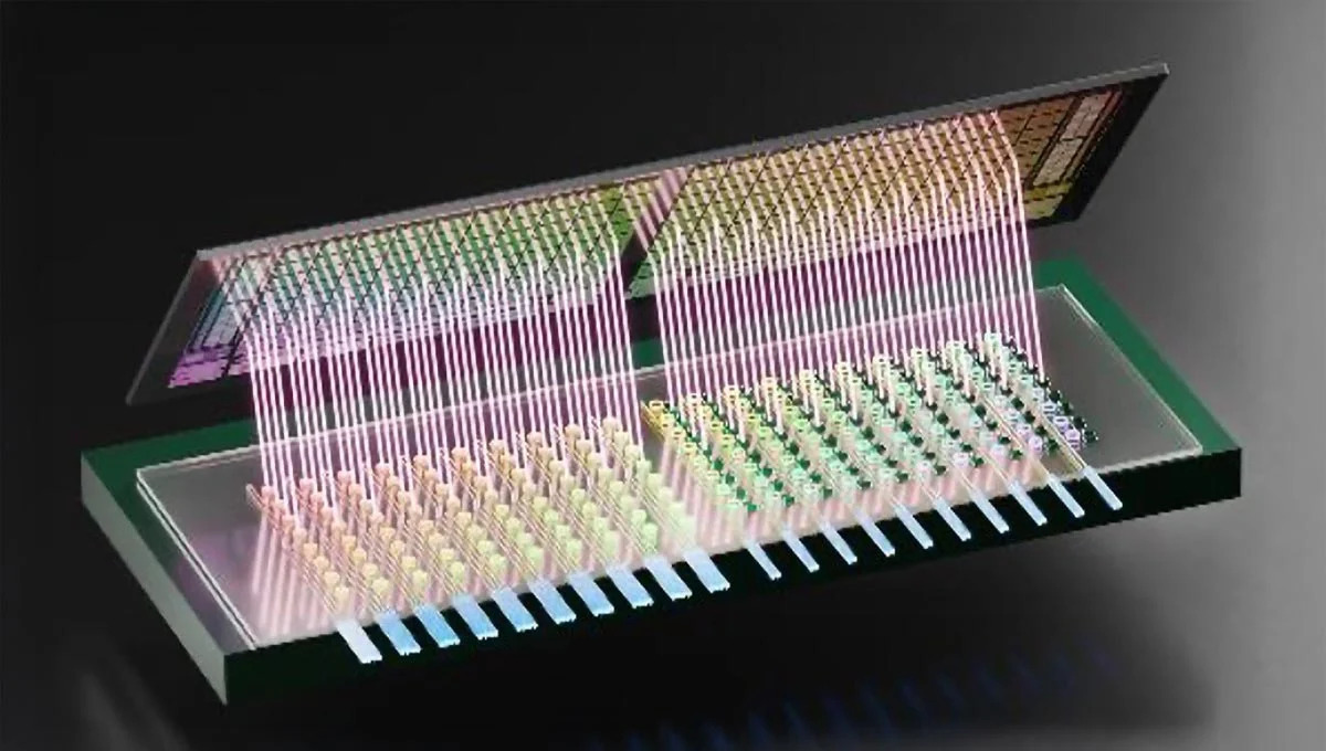
The Columbia Engineering team united with Alyosha Christopher Molnar, Ilda and Charles Lee Professor of Engineering at Cornell University, to evolve a 3D-combined photonic-electronic chip that boasts a high density of 80 photonic transmitters and receivers inside a compact chip footprint. This platform produces high bandwidth (800 Gb/s) with unique energy performance, consuming just 120 femtojoules consistent with bit. With a bandwidth density of 5.3 Tb/s/mm², this development far surpass present benchmarks.
Designed for low price, the chip combines photonic gadgets with CMOS electronic circuits and leverages components produces in industrial foundries, setting the level for widespread industry adoption.
Reshaping AI Infrastructure at the Core
The group’s research redefines how data is transferred among compute nodes, addressing the long-standing bottlenecks in energy performance and scalability. By 3D integrating photonic and electronic chips, this technology attains unrivaled energy savings and excessive bandwidth density, breaking free from traditional data locality constraints. This innovative platform allows AI systems to efficiently transfer large volumes of data, assisting allotted architectures that had been previously impractical because of energy and latency limitations.
Beyond AI: A New Era for Computing
The associated improvement are poised to free up unfamiliar stages of performance, making this technology a cornerstone of destiny computing systems around applications, from huge-scale AI models to actual-time data processing in self independent systems. Beyond AI, this technique holds transformative potential for high-performance computing, telecommunications, and disaggregated memory systems, signaling a new generation of energy-efficient, high-speed computing infrastructure.